


이정철 교수 연구팀, 실리콘 나노입자의 형상과 빛의 방향을 정밀 제어하는 웨이퍼 스케일 제조 기술 개발
2026.07.16
admin

이정철 교수 연구팀(기계공학과·PRISM-AI InnoCORE 연구단)이 실리콘 나노입자의 크기와 형상비를 웨이퍼 단위에서 정밀하게 제어하고, 이를 이용해 빛이 산란되는 방향을 결정론적으로 조절할 수 있는 나노광학 제조 기술을 개발했다. 김태영 박사후연구원이 제1저자로 참여한 이번 연구는 국제학술지 Small에 게재됐으며, 연구의 학술적 우수성을 인정받아 해당 학술지의 후면 표지 (Back Cover) 논문으로 선정됐다.
실리콘과 같은 고굴절률 유전체 나노입자는 입자 내부에서 전기 쌍극자와 자기 쌍극자 공진을 동시에 형성할 수 있다. 두 공진의 세기와 위상이 적절하게 일치하면 뒤쪽으로 산란되는 빛은 억제되고 앞쪽으로 진행하는 빛은 강화되는 Kerker 조건이 구현된다. 이러한 방향성 광산란은 나노안테나, 광검출기, 메타표면, 디스플레이 및 굴절률 센서와 같은 차세대 나노광학 소자의 핵심 원리로 활용될 수 있다.
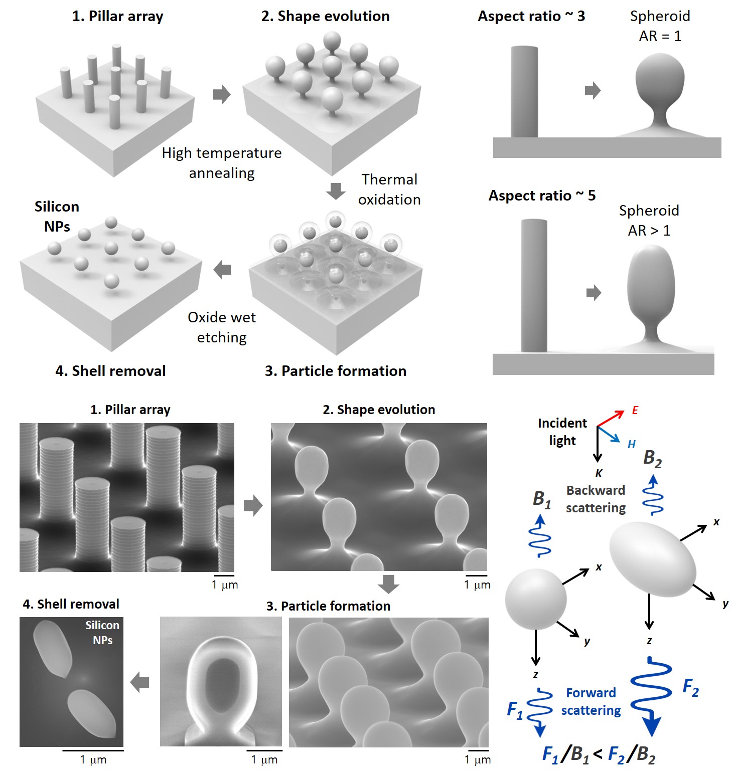
그러나 기존 실리콘 나노입자 제조 방식은 입자의 크기와 형상이 불균일하거나, 구형 이외의 형상을 재현성 있게 제작하기 어렵다는 한계가 있었다. 특히 구형 실리콘 나노입자에서는 전기 쌍극자와 자기 쌍극자 공진이 서로 다른 파장에서 나타나기 때문에, 강한 광산란이 발생하는 공진점에서 두 공진을 정밀하게 중첩시키기 어려웠다. 이에 따라 나노입자의 형상을 설계변수로 이용해 빛의 산란 방향을 안정적으로 제어하는 기술이 요구돼 왔다.
연구팀은 반도체 공정인 리소그래피와 고온 어닐링, 산화를 결합해 실리콘 나노입자의 크기와 형상비를 웨이퍼 규모에서 정밀하게 제어하는 제조 기술을 개발했다. 개발된 공정은 6인치 실리콘 웨이퍼 공정으로 제작할 수 있으며 입자 크기의 변동계수는 1.7–2.4%로 기존 유사 실리콘 나노입자보다 높은 균일도를 나타냈다. 또한 입자의 짧은 축을 일정하게 유지하면서 형상비를 2.1에서 4.0까지 체계적으로 조절해, 원하는 형상의 나노입자를 재현성 있게 제작할 수 있음을 입증했다.
이처럼 정밀하게 제어된 형상은 빛의 산란 방향을 결정하는 핵심 설계변수로 작용했다. 특히 형상비가 2.1인 나노입자에서는 전기 쌍극자와 자기 쌍극자 공진이 중첩되면서 후방 산란은 억제되고 전방 산란은 크게 강화돼, 전방/후방 산란비 12.5를 달성했다. 이는 유사한 기판 및 광학 측정조건에서 보고된 단일 실리콘 나노입자 가운데 가장 높은 수준 중 하나로, 나노입자의 형상만으로 빛의 진행 방향을 결정론적으로 제어할 수 있음을 보여준다.
연구팀은 형상비가 최적화된 나노입자를 단일입자 광학센서로 적용해 높은 굴절률 감도와 6×10⁻⁴ RIU 수준의 검출한계를 확보했다. 또한 혈청 환경에서 나노입자 표면에 단백질 코로나가 형성되는 과정을 무표지 방식으로 실시간 관찰해, 복잡한 생체환경에서도 단백질 흡착의 변화와 속도를 정량적으로 분석할 수 있음을 확인했다.
이번 연구는 불균일한 입자 가운데 적절한 형상을 사후적으로 선택하던 기존 방식에서 벗어나, 목표로 하는 광학적 응답을 갖는 나노입자를 웨이퍼 스케일에서 사전에 설계하고 제조할 수 있는 기반을 마련했다. 개발된 실리콘 나노입자는 저손실 나노안테나, 메타표면, 방향성 광원, 색 구현 소자뿐 아니라 단백질 흡착, 바이러스 결합 및 분자 검출을 위한 무표지 광학센서에도 활용될 수 있다. 또한 동일한 형상비 설계 원리는 저마늄과 SiC 등 다른 고굴절률 유전체 재료에도 확장할 수 있다.
특히 이번 연구는 실리콘 나노입자의 크기와 형상비–전기·자기 쌍극자 공진–전방 산란 특성–굴절률 센싱 성능 사이의 정량적 관계를 실험과 전자기 시뮬레이션으로 규명했다. 또한 동일한 설계값을 갖는 나노입자를 웨이퍼 규모에서 높은 균일도로 구현함으로써, 개별 입자의 광학 응답을 대면적 배열과 메타표면 설계로 확장하기 위한 재현성 있는 나노광학 구성요소를 제시했다. 이러한 형상–광학 응답 데이터는 목표 파장, 색상, 산란 방향 및 센싱 감도에 대응하는 입자 형상과 배열을 탐색하는 AI 기반 메타광학 역설계의 물리적 학습 기반이 된다.
나아가 형상비가 서로 다른 실리콘 나노입자를 조합하면 전기·자기 공진과 빛의 진행 방향을 위치별로 조절하는 메타표면, 방향성 발광소자, 컬러 소자 및 다중 바이오센서로 이어질 수 있다. 본 연구에서 확립한 결정론적 나노입자 제작 기술과 정량적 광학 데이터는 방대한 형상·배열 조합에서 목표 기능에 적합한 구조를 AI가 탐색하고, 이를 실제 웨이퍼급 소자로 구현하는 메타광학 설계–제조 연계의 물리·데이터 기반을 마련했다.
본 연구는 과학기술정보통신부의 InnoCORE 프로그램(N10260002)과 과학기술정보통신부 재원의 한국연구재단 연구과제(RS-2025-00560250, RS-2024-00416835)의 지원을 받아 수행됐다.
논문정보: Kim, T., & Lee, J. (2026). Wafer-scale deterministic fabrication of axis-ratio–engineered silicon nanoparticles for on-resonance electric–magnetic dipole interference. Small, 22(32), e73389. https://doi.org/10.1002/smll.73389
KAIST Research Team Led by Professor Jungchul Lee Develops Wafer-Scale Technology for Precise Control of Silicon Nanoparticle Shape and Directional Light Scattering
A KAIST research team led by Professor Jungchul Lee of the Department of Mechanical Engineering and the PRISM-AI InnoCORE Research Center has developed a wafer-scale nanofabrication technology that precisely controls the size and axis ratio of silicon nanoparticles, enabling deterministic control over the direction of light scattering. Dr. Taeyeong Kim served as the first author. The study was published in Small and selected for the journal’s Back Cover in recognition of its scientific significance.
The team combined semiconductor lithography, high-temperature annealing, and thermal oxidation to fabricate highly uniform spherical and spheroidal silicon nanoparticles across a 6-inch wafer. The particles exhibited a coefficient of variation of only 1.7% – 2.4%, while their axis ratios were systematically tuned from 2.1 to 4.0. This approach overcomes the geometric nonuniformity and limited shape reproducibility of conventional silicon nanoparticle fabrication methods.
Precise shape control allowed the axis ratio to serve as a direct design parameter for optical directionality. At an optimized axis ratio of 2.1, the electric- and magnetic-dipole resonances strongly overlapped, suppressing backward scattering and enhancing forward scattering. The resulting forward-to-backward scattering ratio reached 12.5, among the highest values reported for a single silicon nanoparticle under comparable substrate-supported optical measurement conditions. The optimized nanoparticles also achieved a refractive-index detection limit of 6×10⁻⁴ RIU and enabled real-time, label-free monitoring of protein-corona formation in serum.
The study establishes a quantitative relationship among nanoparticle geometry, electric–magnetic dipole interference, directional scattering, and sensing performance. Combined with the demonstrated wafer-scale uniformity, these results provide reproducible building blocks for large-area metasurfaces, directional light sources, color devices, and multiplexed optical biosensors. The same axis-ratio engineering framework is also applicable to other high-index dielectric materials, including germanium and silicon carbide.
The geometry–optical response relationships established in this work provide a physically grounded basis for AI-driven meta-optical design. The resulting dataset, combining experimental measurements with electromagnetic simulations, provides a physics-based training foundation for the inverse design of nanoparticle geometries and array configurations targeting specific wavelengths, colors, scattering directions, or sensing responses. The work therefore bridges precisely manufactured silicon nanoparticles with AI-guided metasurface design, supporting the development of intelligent nanophotonic and optical sensing platforms.
This research was supported by the Ministry of Science and ICT through the InnoCORE Program (N10260002) and by National Research Foundation of Korea grants funded by the Ministry of Science and ICT (RS-2025-00560250 and RS-2024-00416835).